

|
Electrical Localisation
Scanning Optical
Microscopy
Features:
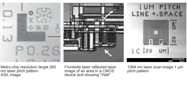
- Multi-laser NIR scanning optical microscope
- 1064 nm laser (capable of electron-hole pair generation through
backside silicon)
- 1340 nm laser (high resolution thermal probe which allows
localized heating)s
- Multiple techniques available (e.g. VBA, TIVA, SDL)
- High power delivery 30 mW at DUT for all objectives including 100x
- Navigation camera for real time backside imaging to complement the
slow scan rate of laser scan module
Application:
Scanned NIR laser activity localize failures which are sensitive to
electron-hole pair generation of thermal stimulation.
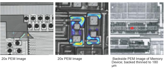
Photon Emission Microscopy
Features:
- High Numerical Aperture (NA)
- Long Working Distance (WD)
- High Sensitivity Macro Lens
- High Sensitivity Detector (Cooled CCD Camera & InGaAs Camera)
- Real Time Backside Imaging
Application:
For localization of detection semiconductor devices caused by leaked
junctions, contact spiking, latch up, oxide breakdown, and other
current leakage phenomenon that produce light emission.
 |