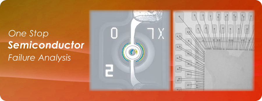


|
Material
Analysis
Scanning Electron
Microscopy (SEM) & Energy Dispersive X-Ray Spectroscopy (EDS)
Analysis
Features:
- 25 Mhz thru-scan
- 15 Mhz, 75 Mhz, 110 Mhz transducers
- Non-destructive inspection method to locate internal
discontinuities in semiconductor package and verify
package reliability
- Detection and verification of complex package designs such as
Stacked Die, encapsulated Flip Chip and Micro
BGA
Specifications:
SEM
- Image Resolution
- 1.5nm or better (at 15 kV)
- 4.0nm or better (at 1 kV)
- Magnification: 20x ~ 500,000x
- Accelerating voltage: 0.5 ~ 30 kV (0.1 kV/step)
EDS
- Elements Detected: B ~ U
- Detection Limits : 0.1 ~ 1 at%
- Depth Resolution : 1 ~ 5 µm
Application:
- Topography Contrast
- Grain Size
- Surface Structure
- Atomic Contrast
- Boundary of two dissimilar elements
- Phase analysis
- Elemental and Chemical Analysis (using energy dispersive x-ray
detector)
- Contamination analysis
X-ray Analysis
Features:
- Resolution 2 µm
- Inspection area 18” x 16” (458x407 mm)
- System magnification up to 2400X for all if inspection area
- Oblique angle 0 to 45 degree for any view 360 degree around a
device
- Data measurement including void percentage, ball diameter,
distance
Sonix Scanning Acoustic Microscope
Features:
- 25 Mhz thru-scan
- 15 Mhz, 75 Mhz, 110 Mhz transducers
- Non-destructive inspection method to locate internal discontinuities in semiconductor package and verify
package reliability
- Detection and verification of complex package designs such as Stacked Die, encapsulated Flip Chip and Micro
BGA
|